The chip industry has spent years telling builders to stop expecting easy hardware gains. Then IBM showed a different escape hatch: stop only shrinking sideways and start building upward.
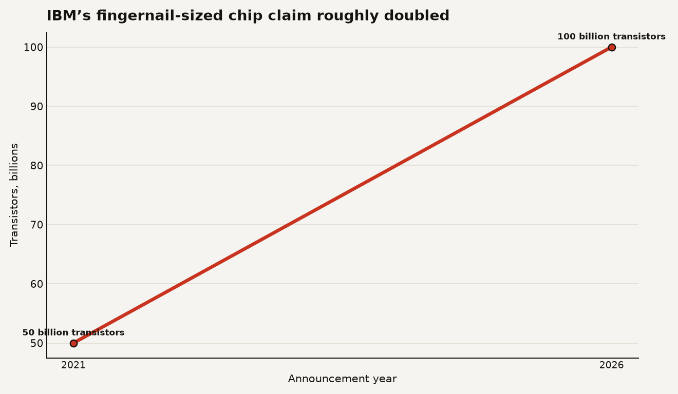
On June 25, 2026, IBM unveiled the IBM nanostack chip, a 0.7 nm, or 7 angstrom, research architecture that packs nearly 100 billion transistors into a fingernail-sized chip. That headline matters because transistor density is the quiet subsidy behind modern AI: every inference batch, vector search pass, model training run, and agent workflow gets cheaper only when silicon keeps improving.
The awkward part: 0.7 nm is a node name, a generation label, and IBM says modern transistor nodes no longer map cleanly to an exact physical dimension. The better way to read the announcement is simpler: IBM claims a path from its 2021 2 nm chip, which fit 50 billion transistors into roughly the same fingernail-sized area, to a stacked design with nearly twice the density.
If you build software, this is still your problem. The AI roadmap is increasingly gated by power, cooling, packaging, memory bandwidth, and capital spending. More transistors help only when the rest of the machine can feed them without cooking the data center. That is the useful lens here: IBM’s nanostack chip is a credible research step, and it is also a reminder that Moore’s Law now needs a construction crane.
What did IBM actually build inside the IBM nanostack chip?
IBM’s new architecture vertically stacks and staggers nanosheet transistors, using 3D sequential integration to put two transistor layers into the same footprint that a conventional planar layout would spread across one layer. IBM describes nanostack as a three-dimensional, nanosheet-based transistor architecture, with staggered NFET and PFET channels that can be optimized independently.
That sounds abstract until you map it to the old chip playbook. For decades, the industry got density by shrinking feature sizes in two dimensions. FinFETs and then gate-all-around nanosheets improved control over current leakage as transistors shrank. Nanostack keeps the nanosheet idea and adds vertical placement. In city terms, IBM is adding another floor because the lot is getting expensive.
The first number to keep in your head is the density jump. IBM’s 2021 nanosheet demonstration put 50 billion transistors on a fingernail-sized chip, and the 2026 nanostack announcement puts the new figure at nearly 100 billion in a similar footprint. The chart below shows the simple version: a five-year move from 50 billion to nearly 100 billion transistors in IBM’s own public milestones.
The second number is performance per watt. A 2025 VLSI paper from IBM researchers projected NanoStack with 4-track base cells at roughly 50 percent iso-power performance improvement or roughly 70 percent iso-performance power reduction versus IBM’s 2 nm node. Those are projections from technical results, so treat them as directionally important and commercially unfinished.
The third number is memory density. IBM says VLSI 2026 research demonstrated 40 percent SRAM scaling for the nanostack architecture, which matters because on-chip memory has become one of the ugly bottlenecks in AI accelerators. More compute without enough local memory creates a very expensive space heater.
There is a big caveat hiding in the node label. IBM’s press release says the 0.7 nm name is a technology generation, while the physical structures still involve nanosheets, bonding layers, channels, contacts, and wiring that do not politely shrink to a literal seven-tenths of a nanometer. For builders, that distinction matters because benchmark-style node numbers are easy to overread. The more important claim is that IBM has shown a manufacturable transistor architecture that can be stacked, connected, and switched.
Why should AI builders care about a research chip that they cannot buy?
Because the bottleneck in AI is moving from model cleverness to infrastructure physics.
The International Energy Agency’s 2026 update projects data center electricity consumption rising from 485 TWh in 2025 to 950 TWh in 2030, while AI-focused data centers triple their consumption over that period. In the same report, the IEA says an advanced AI server rack could reach peak power demand equivalent to 65 households by 2027.
That is the business case for every credible efficiency gain. If a future accelerator could deliver the same work at 70 percent lower chip power, the benefit would show up in more than a spec sheet. It would affect how many racks fit behind a utility interconnect, how much cooling a site needs, how many inference tokens a gross margin can tolerate, and whether your product roadmap assumes more GPUs will always be available next quarter.
For a builder, the consequences land in four places:
- Codebase: kernel efficiency and memory locality will matter more, because denser chips punish software that sprays data across memory tiers.
- Roadmap: hardware refresh assumptions should be explicit, since a 2029 accelerator fleet may have different constraints from a 2026 GPU cluster.
- Costs: power and cooling contracts are becoming part of AI unit economics, not facilities trivia.
- Moat: teams that can tune models, batching, retrieval, and serving around hardware constraints will keep an edge when raw compute is scarce.
There is also a packaging lesson. IBM’s nanostack work is transistor-level 3D integration, which differs from the chiplet and cache stacking you see in commercial products today. AMD’s 3D V-Cache and modern AI packages get a lot of their advantage by stacking dies, memory, or cache around compute. IBM’s claim goes deeper into the transistor layer, which is harder to manufacture but potentially more powerful if yields cooperate.
That last phrase does a lot of work. If either the lower transistor layer or the upper transistor layer fails, the economics can get messy fast. More layers can mean more density, but also more process steps, more thermal constraints, and more ways to lose a die. The production question is less glamorous than the transistor image, and it decides whether this becomes a roadmap or a museum photo.
What has to happen before nanostack reaches real data centers?
IBM says it sees a path to production in as early as the next five years for sub-1 nm nanostack technology. That is an optimistic but useful marker: think early 2030s for broad relevance, with elite products first and mainstream trickle-down later.
The manufacturing stack has to mature around the architecture. IBM and Lam Research announced a five-year collaboration on March 10, 2026 to develop materials, fabrication processes, High NA EUV techniques, nanosheet and nanostack devices, and backside power delivery. That is the part of the story that makes the transistor claim less lonely. IBM is building the process ecosystem, not just publishing a pretty cross-section.
High NA EUV is one of the expensive gates. ASML and Intel said in 2022 that Intel ordered the first TWINSCAN EXE:5200 high-volume production system, with more than 200 wafers per hour productivity. Data Today has covered why that tool class turns advanced chips into a capital bottleneck for AI hardware, because even brilliant transistor ideas need lithography capacity before they become chips you can deploy.
Foundry timing matters too. TSMC’s 2025 annual report says its 2 nm technology entered high-volume manufacturing in the fourth quarter of 2025, with N2P and A16 scheduled for volume production in the second half of 2026. That means IBM’s nanostack announcement sits ahead of today’s commercial leading edge. It is a signal about the post-2 nm path, not a replacement for the N2 products hitting roadmaps now.
The practical checklist is short:
- Can nanostack yields survive real product die sizes, not just test structures?
- Can thermal budgets stay low enough while adding layers above finished devices?
- Can SRAM, logic, interconnect, and power delivery improve together rather than in separate slides?
- Can foundries absorb the process complexity without blowing up wafer costs?
If you are planning AI infrastructure, the action is boring and valuable: model power as a first-class constraint. Do not assume a transistor breakthrough cancels the need for better quantization, routing, caching, batch scheduling, retrieval pruning, and model selection. Silicon gains usually arrive unevenly. Software that wastes the first generation of new hardware will pay full price for half the benefit.
How should you change your roadmap now?
Start by separating procurement from architecture planning. You cannot buy an IBM nanostack chip for your 2026 cluster, but you can design systems that benefit from denser, more memory-sensitive accelerators when they arrive.
For application teams, that means building observability around tokens, memory movement, cache hit rates, queueing delay, and utilization. A 50 percent performance gain at the transistor level does not automatically become a 50 percent gain in your product if your bottleneck is retrieval latency, network hops, storage reads, or a badly packed serving queue.
For founders, the lesson is to be skeptical of “compute will get cheaper” as a complete strategy. It probably will in some dimensions. It may also get more capital-intensive, more capacity-constrained, and more geographically tied to power availability. The IEA’s 2030 projection of 950 TWh for data centers is the macro version of your cloud bill: demand is rising fast enough that efficiency improvements can be swallowed by usage growth.
For infrastructure buyers, keep three dates on the whiteboard. TSMC says N2 entered high-volume manufacturing in 4Q 2025. IBM says nanostack has a path to production in as early as five years from June 2026. IBM and Lam’s process collaboration runs for five years from March 2026. Those dates put nanostack in the strategic planning window, not the current purchasing window.
The best near-term bet is to make your stack hardware-adaptive. Use abstraction where it helps, but keep the performance-critical pieces inspectable. Treat every model serving path as something that may need to be retuned for a new memory hierarchy, a new accelerator topology, or a new chiplet package. If your AI system only works on one vendor’s current GPU shape, you are renting more of your roadmap than you think.
Moore’s Law now has stairs
IBM’s nanostack chip does not make the physics problem disappear. It changes the shape of the bet.
The old version of Moore’s Law felt like a metronome: wait, refresh hardware, enjoy cheaper compute. The next version looks more like civil engineering. It needs stacked devices, High NA EUV, backside power, advanced packaging, memory scaling, liquid cooling, and power contracts to move together.
That is messier. It is also where the advantage moves. Builders who understand the hardware curve early will write software that rides it. Everyone else will discover, one invoice at a time, that nearly 100 billion transistors still need somewhere to plug in.
Sources
- IBM Newsroom: IBM Debuts World’s First Sub-1 Nanometer Chip Technology
- IBM Research: NanoStack Transistor Architecture for CMOS 7A Node and Beyond
- IBM Research: Introducing the world’s first 2 nm node chip
- IBM Newsroom: IBM and Lam Research Announce Collaboration to Advance Sub-1nm Logic Scaling
- IEA: Key Questions on Energy and AI, executive summary
- TSMC: 2025 Annual Report
- ASML: Intel and ASML strengthen their collaboration to drive High-NA into manufacturing in 2025