The most important AI hardware story this week is a machine almost no builder will ever touch. It weighs more than a small fleet of cars, costs as much as a startup round you would frame on the wall, and decides how many future accelerators can exist.
That machine is ASML’s High-NA EUV scanner. MIT Technology Review’s June 23, 2026 feature puts the going price at $400 million per tool and describes a 150-ton system built to print smaller chip features for the next wave of AI silicon in its report from ASML’s Veldhoven site. The useful read for builders is simple: High-NA EUV is the 8 nm lithography step that can push denser AI chips forward, while turning the chip supply chain into an even narrower capital gate.
If you build on GPUs, rent GPUs, sell AI features, or plan around model costs, this matters. Your roadmap already depends on fabs, packaging, HBM, power, and cooling. As we argued in the AI factory cooling fight, the bottleneck keeps moving down the stack. High-NA EUV moves it into the cleanroom optics.
What did ASML actually ship, and why is 8 nm the number to care about?
ASML’s new production platform is the TWINSCAN EXE line, a High-NA EUV system that raises numerical aperture from the 0.33 NA used by its NXE EUV tools to 0.55 NA according to ASML’s EUV product documentation. In plain English, the optics collect and focus the 13.5 nm EUV light more tightly, which lets fabs print smaller features without leaning as hard on repeated patterning steps.
The key spec is brutal in its simplicity. ASML says the TWINSCAN EXE:5200B reaches 8 nm resolution, compared with 13 nm on its NXE systems, and that this lets chipmakers print features 1.7 times smaller in a single exposure on the EXE:5200B product page. The same ASML page says the platform can enable transistor densities 2.9 times higher than those possible with TWINSCAN NXE systems in a single exposure.
The chart below shows the scale of the optical jump: 13 nm on NXE low-NA EUV falls to 8 nm on EXE High-NA EUV, while ASML’s claimed single-exposure density uplift rises to 2.9 times.
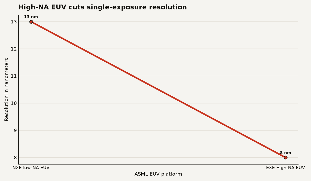
That shrink is the part buyers care about, but the production story is messier. ASML says EXE systems are intended to support high-volume manufacturing in the 2025 to 2026 window and geometric scaling into the next decade in its EUV systems overview. The company also says the first High-NA EUV system was delivered in December 2023, which means the industry is only a few years into learning the full process stack around the tool.
High-NA also changes the surrounding workflow. ASML and imec opened a joint High NA EUV Lithography Lab in Veldhoven on June 3, 2024 to give logic, memory, materials, and equipment companies access to a prototype scanner plus surrounding coat, development, metrology, wafer handling, and mask handling tools in their lab announcement. That list is the warning label. A lithography scanner never arrives alone. It drags process chemistry, masks, inspection, computational lithography, and design rules behind it.
Why does a $400 million lithography tool change your AI roadmap?
The wrong response is to treat High-NA EUV as a magic density knob. The better response is to treat it as a capital allocation signal from the companies that decide your hardware curve.
ASML’s own business is already leaning into that signal. The company reported €32.7 billion in 2025 net sales and €9.6 billion in net income in its full-year 2025 results. In Q1 2026, ASML reported €8.8 billion in net sales and raised its 2026 revenue outlook to €36 billion to €40 billion in its April 15, 2026 results.
Those numbers matter because advanced AI capacity expands only when capex clears several gates at once. A cloud provider can want more accelerators. Nvidia, AMD, Broadcom, or a custom silicon team can tape out a stronger chip. None of that creates inventory unless foundries can buy tools, qualify processes, secure masks and resists, package the dies, and power the data centers.
For you, the practical consequences are less glamorous than the physics:
- Roadmap timing gets tied to fab insertion. If a model feature depends on cheaper next-generation inference, you are really betting on process ramps, packaging capacity, and yield curves across 2026 to 2029.
- Unit economics inherit tool economics. A $400 million scanner has to earn its place through fewer process steps, higher wafer output, better yield, or chips that command enough margin to cover the pain.
- Moats shift toward supply commitments. A startup cannot out-prompt a competitor that has reserved compute years ahead, unless its product needs far less compute per dollar of revenue.
- Hiring changes shape. Teams that understand compiler efficiency, memory traffic, batching, quantization, and workload placement become cheaper than blindly buying more tokens at peak GPU prices.
ASML’s technology pitch is that High-NA can reduce process complexity by using single exposure where older approaches require multiple patterning on the EXE:5000 product page. That is the part that can offset the sticker shock. Fewer steps can mean shorter cycle time, fewer opportunities for defects, and more wafer output from a fab line that is already packed with expensive tools.
The business catch is adoption order. ASML and Intel announced in January 2022 that Intel had placed the first purchase order for the industry’s first TWINSCAN EXE:5200 system, described as a High-NA EUV high-volume production system with more than 200 wafers per hour productivity in the joint ASML release. That was a strategic bet by Intel, not a guarantee that every leading foundry would move at the same moment.
If you are planning AI costs, that distinction matters. A new lithography generation can be both technically inevitable and commercially staggered. The first customers absorb integration pain. Later customers benefit from recipes, materials, metrology, and operator learning that were not free.
How much of this is a monopoly problem rather than a chip problem?
ASML is the only supplier of complete EUV lithography systems, and its own EUV overview says EUV technology is unique to ASML in the company’s product materials. That is why this story lands differently from a normal component launch. If one GPU vendor has a shortage, another chip or cloud route may help. If the leading-edge lithography route is constrained, the whole advanced-node map tightens.
Export controls make the bottleneck political. The U.S. Bureau of Industry and Security said its October 7, 2022 controls restricted China’s ability to both purchase and manufacture certain high-end chips and covered semiconductor manufacturing equipment in the Commerce Department release. The Netherlands expanded its national export control measure for advanced semiconductor manufacturing equipment as of September 7, 2024, specifically naming deep ultraviolet lithography equipment as the targeted technology in the Dutch government notice.
The key builder lesson is that advanced compute supply now sits inside trade policy. That means procurement risk can arrive from a government notice as easily as from a bad yield report.
There are challengers, but the burden of proof is high. Substrate says it is building next-generation U.S. fabs powered by advanced X-ray lithography on its company purpose page. The U.S. Commerce Department and NIST finalized $150 million in CHIPS incentives for xLight on June 2, 2026 to demonstrate a free-electron laser prototype as an alternative EUV light source in the NIST award announcement.
Those efforts are worth watching because they attack the right choke point: light. They also face the same ugly checklist ASML spent decades grinding through: source power, optics, masks, resists, metrology, uptime, overlay, throughput, serviceability, and customer trust. A lab result earns attention. A fab tool earns a purchase order only after it can run all day without turning yield into confetti.
What should builders do before High-NA EUV hits their cloud bill?
Start by separating two clocks. The physics clock says High-NA EUV gives the industry a path to smaller features and higher density. The product clock says your AI feature will feel the benefit only after fabs qualify nodes, chip vendors tape out products, packaging capacity scales, cloud vendors buy inventory, and pricing reaches your workload.
That lag is where bad planning happens.
If you run an AI product, do three things now. First, benchmark the revenue sensitivity of your model cost at 2 times and 4 times today’s inference price, because supply shocks rarely ask permission. Second, keep a smaller model path alive, even if the frontier model demos better, because efficient fallback is a margin tool. Third, write vendor contracts with more than one compute route where possible, because lithography, HBM, networking, and power can each become the limiting reagent.
If you build infrastructure, read High-NA as a reason to invest in efficiency rather than a reason to wait for cheaper chips. Better batching, KV cache management, speculative decoding, quantization, routing, and workload-aware scheduling pay off whether the next node arrives on time or slips. A team that cuts inference cost by 30 percent has created its own mini node shrink without waiting for a 150-ton machine to clear customs.
If you sell to enterprises, expect procurement teams to ask harder questions about compute exposure. Buyers already worry about data risk, security, and vendor lock-in. They will increasingly ask whether your gross margin collapses when GPUs get scarce or cloud discounts expire. You need an answer that sounds like an operating plan, not a shrug wrapped in a benchmark slide.
The caveat is important: High-NA EUV does not automatically mean cheaper AI. It means the semiconductor industry has another scaling tool at a time when demand for compute is enormous. Prices depend on yield, competition, utilization, packaging, memory, power, and how much margin every layer in the stack can keep.
The bottleneck has a bill of materials
A $400 million lithography machine is easy to mythologize because it looks like science fiction with a purchase order. The sharper view is less romantic. High-NA EUV is a dependency graph made of mirrors, lasers, tin droplets, vacuum chambers, export licenses, process recipes, and balance sheets.
For builders, the lesson is uncomfortable and useful: AI does not run on vibes. It runs on fabs. The next time a roadmap assumes compute will simply get cheaper, ask which machine prints that assumption.
Sources
- MIT Technology Review: The $400 million machine powering the future of chipmaking
- ASML: TWINSCAN EXE:5200B product page
- ASML: EUV lithography systems overview
- ASML: TWINSCAN EXE:5000 product page
- ASML: Q4 and full-year 2025 financial results
- ASML: Q1 2026 financial results
- ASML: Intel and ASML strengthen their High-NA collaboration
- ASML: ASML and imec open High NA EUV Lithography Lab
- U.S. Bureau of Industry and Security: Commerce implements China semiconductor controls
- Government of the Netherlands: Export control measure for advanced semiconductor manufacturing equipment
- Substrate: Our purpose
- NIST: Commerce finalizes CHIPS incentives with xLight